1–3 μm Au bond pads on a 150 mm SiC wafer.
At 10–25% deposition utilization, 75–90% of your Au is ending up on chamber walls. That math scales with production.
The SiC MOSFET market is projected to grow 10× by 2035.
Gold is at $4,800 an ounce.
Those two trends are on a collision course inside every fab running thick Au bond pad metallization.
The math:
A 150 mm SiC wafer with 1–3 μm Au bond pads carries 0.1–0.4 grams of gold per wafer.
At typical e-beam utilization without optimization, a significant portion of that spend never reaches the device.
At $4,800/oz, that shows up in the P&L. And this isn’t scaling linearly.
Wafer starts are increasing. Wafer diameter is moving from 150 mm to 200 mm, expanding the bond pad area per wafer.
Programs are locking in long-term supply commitments.
The inefficiency you carry today becomes the cost you carry for the next decade, and it comes down to geometry.
E-beam vapor follows a cosine-law distribution. In static planetary systems, wafers at the edge receive less flux.
So you either:
• over-deposit to compensate
• or accept thinning, and the reliability risks that follow
The alternative is motion geometry.
Dual-axis planetary systems, combined with vapor cloud optimization, are designed to intercept a greater fraction of evaporated material, reducing Au consumption by up to 40% (EP2766921B1).
At $4,800/oz and 10× volume growth, that improvement compounds quickly.
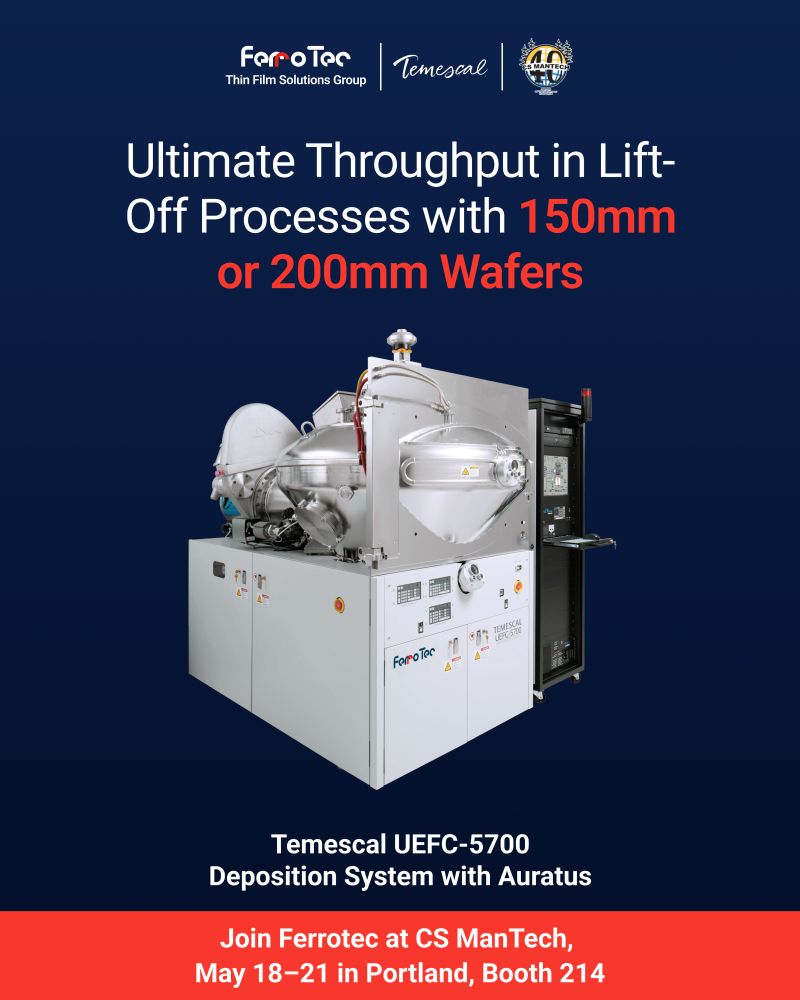
CS MANTECH is happening May 18–21 in Portland. Find Ferrotec (Thin Film Solutions Group) at booth 214. Let’s discuss this and more.
Wolfspeed | Infineon Technologies | onsemi | STMicroelectronics | RTX
#SiC MOSFET #gold bond pads #semiconductor fab #e-beam deposition #CS MANTECH
At 10–25% deposition utilization, 75–90% of your Au is ending up on chamber walls. That math scales with production.
The SiC MOSFET market is projected to grow 10× by 2035.
Gold is at $4,800 an ounce.
Those two trends are on a collision course inside every fab running thick Au bond pad metallization.
The math:
A 150 mm SiC wafer with 1–3 μm Au bond pads carries 0.1–0.4 grams of gold per wafer.
At typical e-beam utilization without optimization, a significant portion of that spend never reaches the device.
At $4,800/oz, that shows up in the P&L. And this isn’t scaling linearly.
Wafer starts are increasing. Wafer diameter is moving from 150 mm to 200 mm, expanding the bond pad area per wafer.
Programs are locking in long-term supply commitments.
The inefficiency you carry today becomes the cost you carry for the next decade, and it comes down to geometry.
E-beam vapor follows a cosine-law distribution. In static planetary systems, wafers at the edge receive less flux.
So you either:
• over-deposit to compensate
• or accept thinning, and the reliability risks that follow
The alternative is motion geometry.
Dual-axis planetary systems, combined with vapor cloud optimization, are designed to intercept a greater fraction of evaporated material, reducing Au consumption by up to 40% (EP2766921B1).
At $4,800/oz and 10× volume growth, that improvement compounds quickly.
CS MANTECH is happening May 18–21 in Portland. Find Ferrotec (Thin Film Solutions Group) at booth 214. Let’s discuss this and more.
Wolfspeed | Infineon Technologies | onsemi | STMicroelectronics | RTX
#SiC MOSFET #gold bond pads #semiconductor fab #e-beam deposition #CS MANTECH
Shared byJamie Diaz - 22 days ago
Log in to comment
Loading ..
Related Articles
Ferrotec Teams Unite: Europe and USA Collaborate in Bedford

Introducing Dr. Sadaf Khan: Shaping Ferrotec Life Sciences' Future

Understanding and Mitigating UBM Stack Failures in Compound Semiconductor Manufacturing

Discover High-Throughput Metallization with Temescal UEFC-5700 System

Ferrotec Leaders Visit Ferrotec USA: Strengthening Global Collaboration

Revolutionize Electron Beam Deposition with HULA Technology
11
0/100